All solutions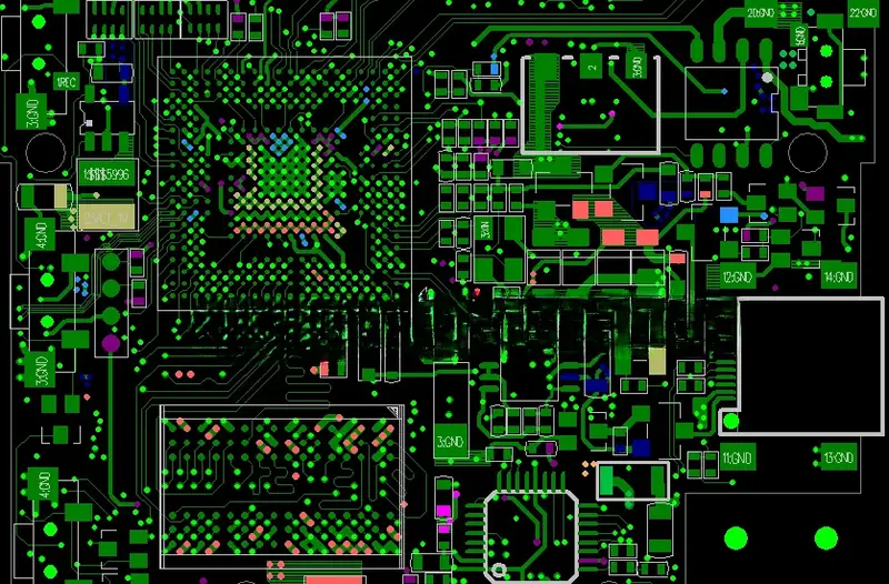
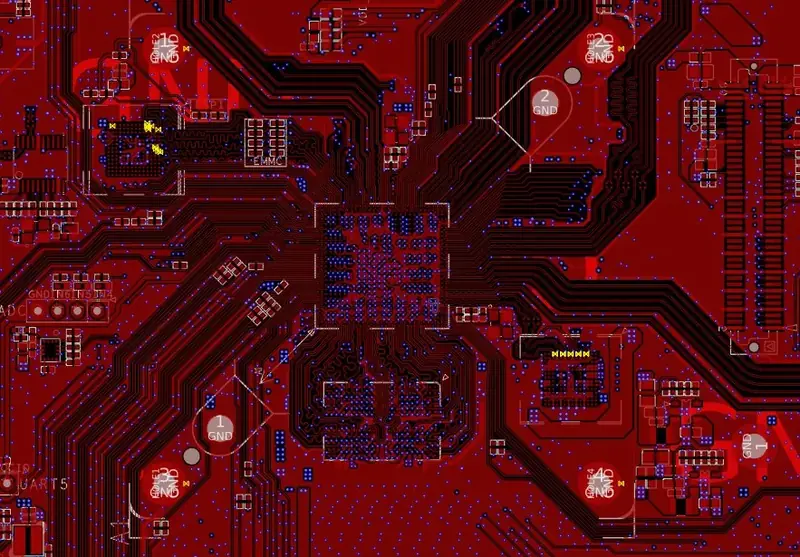
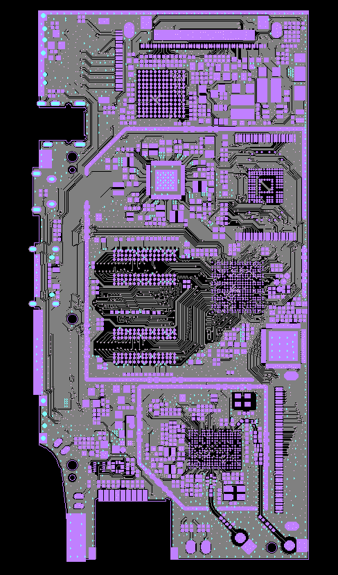
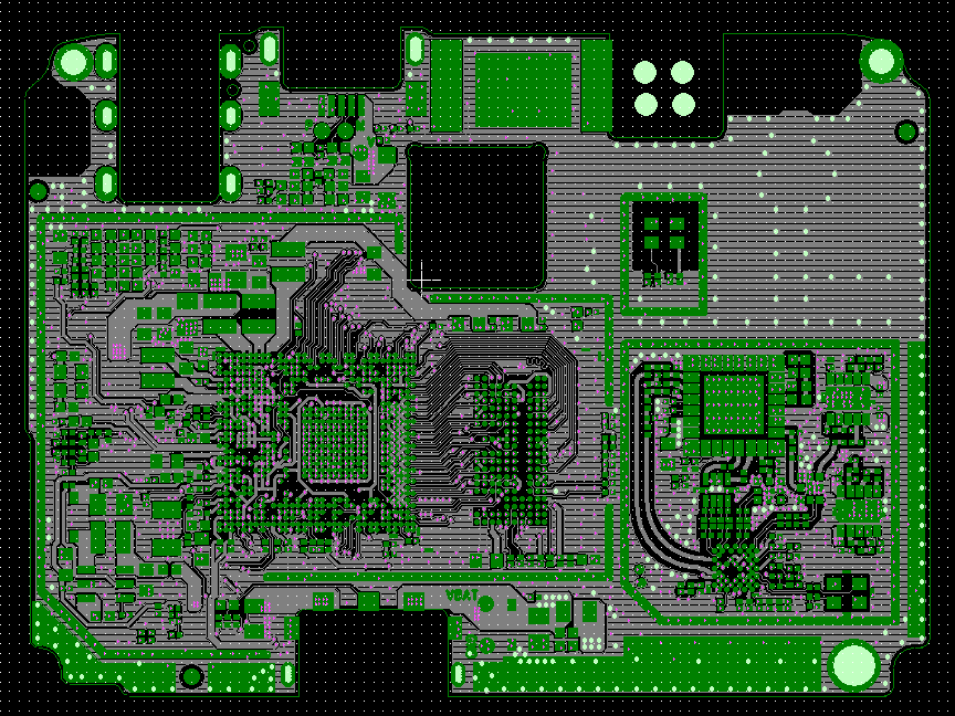
Custom PCB Layout
Precision PCB layout for high-density, high-reliability boards
High-quality layout with SI, PI and DFM in mind.
Customer pain points
Common challenges we solve
- ✕Tight mechanical envelopes and dense routing
- ✕High-speed signals requiring impedance control
- ✕Power integrity and thermal hotspots
- ✕Boards that fabricate but fail assembly or test
What CC Circuits does
Our approach
Stack-up planning and impedance-controlled routing
High-speed, RF and mixed-signal layout
Power distribution, thermal relief and EMI considerations
DFM/DFA review with fabrication and assembly teams
Real cases
Layout case examples